First images and spectra of individual carbon nanotubes in a general environment
November 14, 2013

In
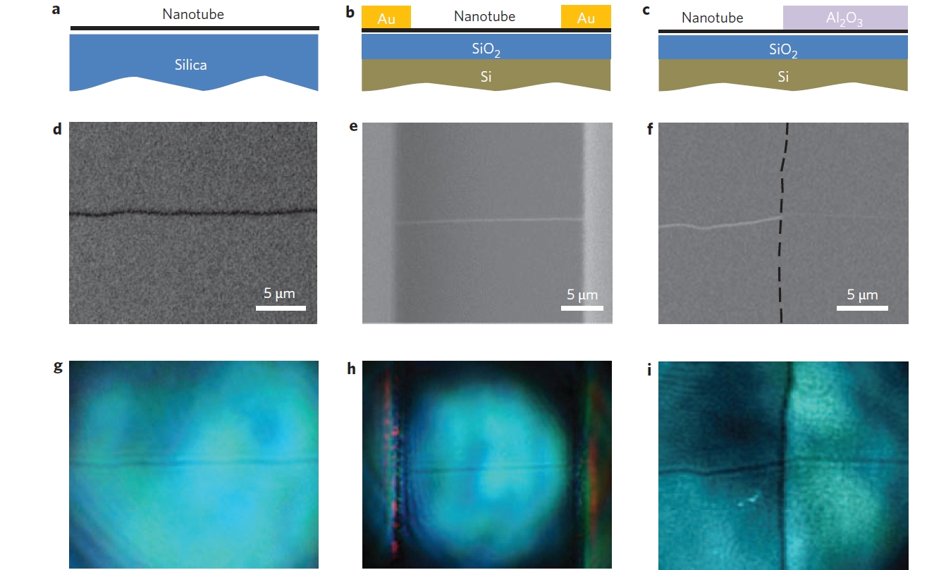
this display showing optical imaging and spectroscopy of an individual
nanotube on substrates and in devices, (a-c) are schematics of a
nanotube on a fused-silica substrate, in a field-effect transistor
device with two gold electrodes, and under an alumina dielectric layer;
(d-f) are SEM images and (g-i) are direct optical images of these
individual nanotubes (credit: Feng Wang/Lawrence Berkeley National
Laboratory)
The physical structure and electronic properties of each individual species of single-walled carbon nanotubes are governed by chirality, meaning their structure has a distinct left/right orientation or “handedness.”
So achieving chirality-controlled growth of carbon nanotubes and understanding the physics behind chirality-dependent devices are two of the biggest challenges in nanotube research.
Also, a single-walled carbon nanotube can be metallic or semiconducting depending on its exact structure. Semiconducting nanotubes can have very different electronic bandgaps, resulting in wildly different electronic or optical properties.
“Using a novel high-contrast polarization-based optical microscopy set-up, we’ve demonstrated video-rate imaging and in-situ spectroscopy of individual carbon nanotubes on various substrates and in functional devices,” says Feng Wang, a condensed matter physicist with Berkeley Lab’s Materials Sciences Division.
How to image an individual nanotube
“For the first time, we can take images and spectra of individual nanotubes in a general environment, including on substrates or in functional devices, which should be a great tool for advancing nanotube technology.”
“Polarization-based optical microscopy and spectroscopy techniques are well-suited for meeting these challenges, as polarized light is extremely sensitive to optical anisotropy in a system and has long been exploited to study chirality in molecules and crystals,” Wang says. “However, the small signal and unavoidable environment background has made it difficult to use polarized optical microscopy to study single carbon nanotubes.”
Difficulties arise from an apparent contradiction in polarization-based optical microscopy. For any optical microscope, a large numerical aperture (NA) objective is crucial for high-spatial resolution, but polarized light passing through a large NA objective becomes strongly depolarized. With their new technique, Wang and his colleagues were able to do what has not been done before and simultaneously achieve both high polarization and high spatial resolution.
“The key to our success was the realization that light illumination and light collection can be controlled separately,” Wang says. “We used a large NA objective for light collection to obtain high spatial resolution, but were able to create an effectively small NA objective for illumination to maintain high polarization purity.”
“We observed that high order nanotube optical resonances are dramatically broadened by electrostatic doping, an unexpected behavior that points to strong inter-band electron-electron scattering processes dominating the ultrafast dynamics of excited states in carbon nanotubes,” Wang says.
In addition to individual single-walled carbon nanotubes, Wang and his colleagues say their technique can also be used to greatly enhance the optical contrast of other anisotropic (irregular) nano-sized materials that are “invisible” to conventional optical microscopes, including graphene nanoribbons, semiconductor nanowires and nanorods, and nanobiomaterials such as actin filaments.
This research was supported by grants from the National Science Foundation, the Center for Integrated Nanomechanical Systems, and by DOE’s Office of Science.
Abstract of Nature Nanotechnology paper
Single-walled carbon nanotubes are uniquely identified by a pair of chirality indices (n,m), which dictate the physical structures and electronic properties of each species. Carbon nanotube research is currently facing two outstanding challenges: achieving chirality-controlled growth and understanding chirality-dependent device physics. Addressing these challenges requires, respectively, high-throughput determination of the nanotube chirality distribution on growth substrates and in situ characterization of the nanotube electronic structure in operating devices. Direct optical imaging and spectroscopy techniques are well suited for both goals, but their implementation at the single nanotube level has remained a challenge due to the small nanotube signal and unavoidable environment background. Here, we report high-throughput real-time optical imaging and broadband in situ spectroscopy of individual carbon nanotubes on various substrates and in field-effect transistor devices using polarization-based microscopy combined with supercontinuum laser illumination. Our technique enables the complete chirality profiling of hundreds of individual carbon nanotubes, both semiconducting and metallic, on a growth substrate. In devices, we observe that high-order nanotube optical resonances are dramatically broadened by electrostatic doping, an unexpected behaviour that points to strong interband electron-electron scattering processes that could dominate ultrafast dynamics of excited states in carbon nanotubes.
(¯`*• Global Source and/or more resources at http://goo.gl/zvSV7 │ www.Future-Observatory.blogspot.com and on LinkeIn Group's "Becoming Aware of the Futures" at http://goo.gl/8qKBbK │ @SciCzar │ Point of Contact: www.linkedin.com/in/AndresAgostini
 Washington